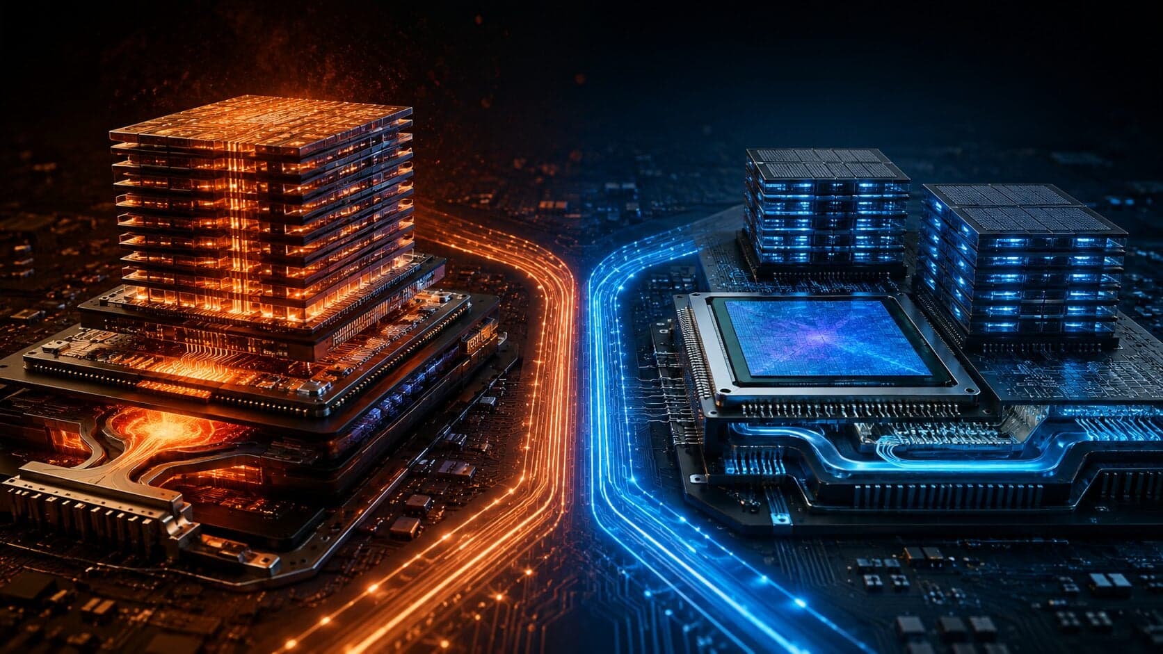
For decades, semiconductor progress was told through the story of the chip itself. That story still matters — but it no longer explains how the most advanced AI systems get faster. The most consequential change is now happening around the die as much as inside it.
In Beyond the Die: The Definitive Guide to Advanced Packaging in the AI Era, Techstrong Group CEO Alan Shimel lays out why leading AI accelerators are no longer chips but systems — logic dies, HBM stacks, interposers, substrates, power delivery, thermal engineering, and increasingly co-packaged optics, all inside one enormous package. Produced in partnership with the analyst team at Futurum Group, the report draws on Futurum Intelligence’s 1H 2026 data center semiconductor forecast and a survey of 824 decision-makers to map where the real constraints live.
What’s Inside
- Why “packaging is the bottleneck” is directionally right but incomplete — and how the binding constraint moves between CoWoS interposers, HBM, substrates, bonding yield, test, power, and networking every 12–18 months
- A practical guide to 2.5D, 3D, and fan-out — including TSMC’s CoWoS-S, -R, and -L variants and the 5.5×-reticle platform certified in 2025
- How HBM4’s custom logic base die is fusing memory into accelerator architecture — and where Samsung, SK hynix, and Micron each sit
- Chiplets and UCIe 3.0: what’s shipping vs. what’s still promised
- Co-packaged optics from Broadcom’s Tomahawk 6-Davisson, NVIDIA’s Spectrum-X and Quantum-X, and Marvell
- The OSAT landscape — ASE, Amkor’s $1.5B NVIDIA deal, JCET, and PTI — and what to watch through 2028
The package is no longer what surrounds the computer. Increasingly, the package is the computer. Download the full report below.