China has been working to circumvent the highly restrictive sanctions related to chip technology that the US put in place starting in 2019, and now it may have achieved that in the form of a breakthrough with semiconductor giant Huawei.
The chip giant, specifically named in the 2019 sanctions, said this week that it had achieved a fabrication breakthrough that would allow it to make cutting-edge chips on par with TSMC and Intel within five years.
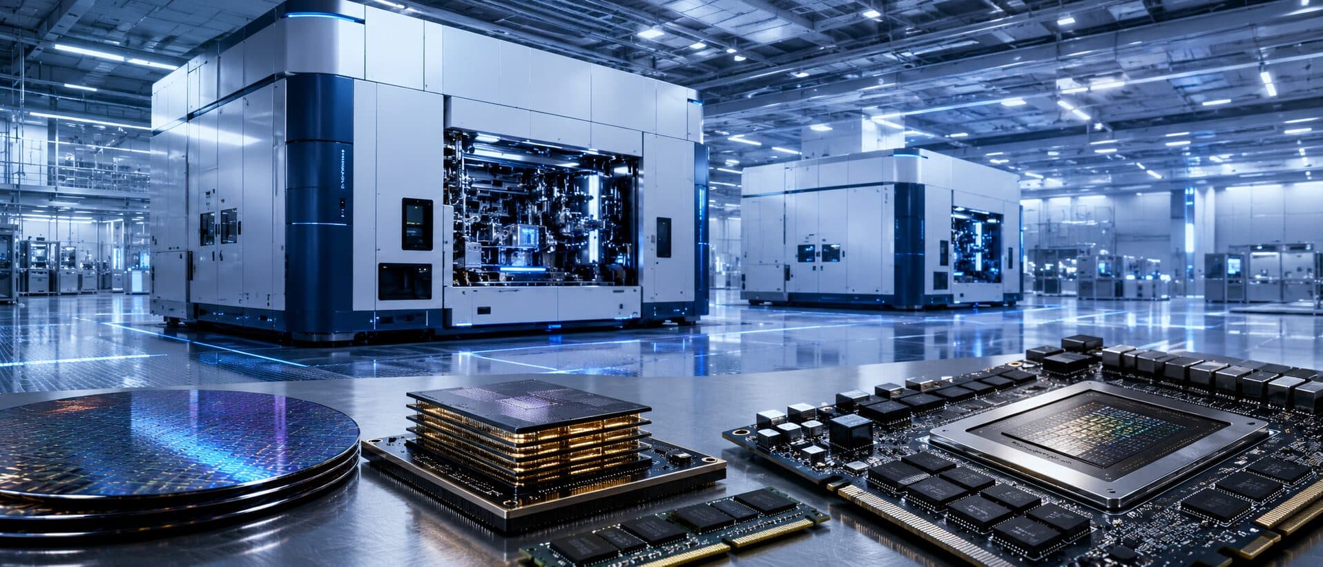
With the United States and China vying for global dominance in artificial intelligence, U.S. sanctions that began in 2019 have largely cut Huawei off from global makers of semiconductor chips, the tiny brains that power everything from smartphones to computers to cars.
China has been desperately trying to find a way around Washington’s limits, which has effectively shut Huawei out of working with TSMC even as it routinely threatens Taiwan with invasion. With Beijing’s access to chip design software and semiconductor manufacturing equipment, such as advanced lithography machines, restricted, the Chinese government’s solution has been to invest in developing its own semiconductor supply chain.
Huawei said at a tech conference in Shanghai that by 2031, its high-end chips would have transistor density equivalent to 1.4-nanometer processes, which is considered the industry’s cutting edge. TSMC is expected to reach mass production volume of 1.4NM by 2028 and Intel is expected to reach it by 2029.
That puts Huawei a little bit behind TSMC and Intel, but not by much, and it’s a lot better than the disparity now. Intel is ramping up production of 1.8 NM while TSMC is using 2 NM, and Huawei is left in the dust with 7 NM for its most advanced processing nodes.
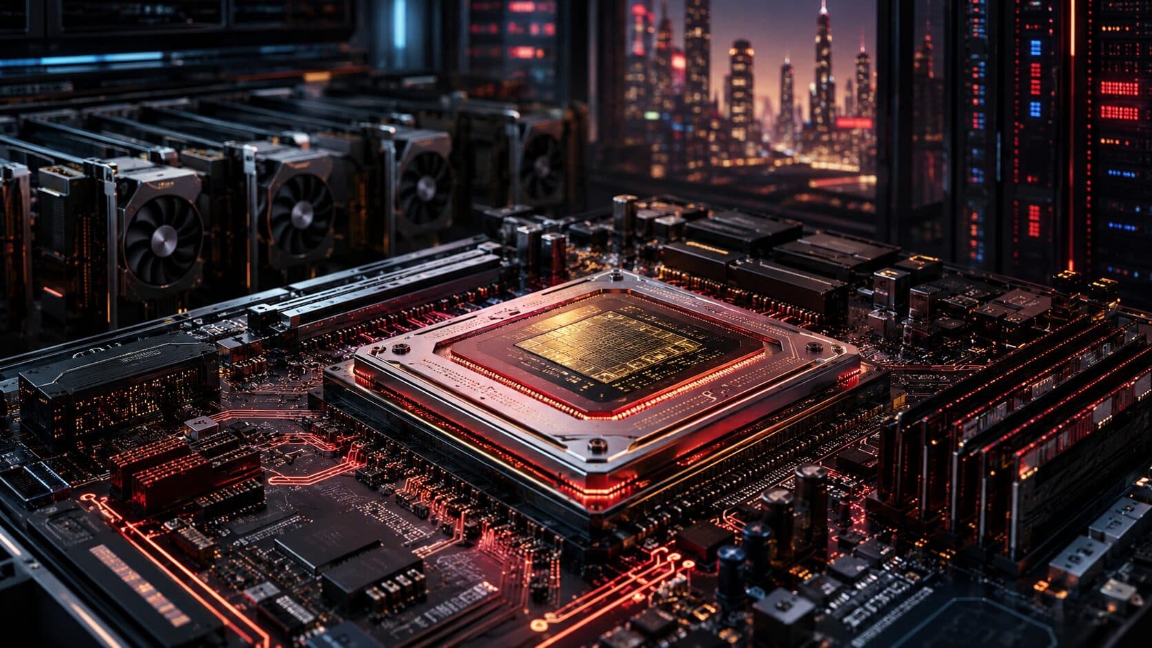
Huawei’s president of semiconductor business He Tingbo said in a speech that Huawei calls the breakthrough “LogicFolding,” to be used in its future Kirin chips. Rather than achieving performance gains by shrinking transistors as Intel and TSMC do, Huawei is folding traditional 2D circuits into 3D vertically stacked semiconductors, a common technique used by memory makers, essentially creating chip “skyscrapers” by stacking chips on top of each other.
Huawei calls this new design the Tau Scaling Law, which reduces the time it takes data to move through chips by stacking them rather than spreading the transistors in a 2D design.
“Cost, power, heat and system integration remain major challenges, especially for Cloud AI services,” Brady Wang, associate director at Counterpoint Research, told Reuters. “In the short term, China may narrow the gap with global leaders, but a technology gap with the most advanced nodes will still remain.”
Originally published by Techstrong.IT. Republished with attribution.