Intel appears to be rethinking a key element of its semiconductor strategy as interest emerges from outside companies in its advanced 18A manufacturing process. The shift comes less than a year after CEO Lip-Bu Tan signaled that the technology might be reserved largely for Intel’s own products.
Chief Financial Officer David Zinsner reportedly said the company now sees potential in offering the 18A node to external customers through its foundry services. The reassessment follows technical progress in the process and inquiries from potential partners evaluating the technology.
The 18A process, roughly equivalent to a 1.8-nanometer class manufacturing node, is among Intel’s most ambitious fabrication efforts. When Tan assumed leadership in early 2025, he questioned whether it made business sense to market the technology broadly to outside clients. Over the past year, however, Intel says production improvements have changed the company’s outlook, so the 18A process could be offered to customers.
Potential Customers
Interest has reportedly focused on a variant known as 18A-P, which is designed to deliver higher performance and energy efficiency compared with the base process. While Intel has not named any companies evaluating the node, executives indicated that discussions with potential customers are underway.
Even with these improvements, the technology remains in an early stage. Intel says the manufacturing process is still maturing as production ramps up, with yields expected to improve over time. Such challenges are not unusual for cutting-edge fabrication technologies.
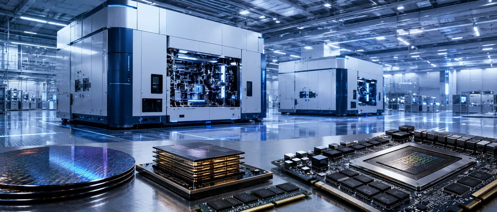
The 18A process introduces two major innovations: gate-all-around RibbonFET transistors and a backside power delivery system. Both technologies promise higher efficiency and performance but add significant complexity to the manufacturing process.
Intel expects yields to improve steadily over the coming year as production ramps up. The company has already begun using the process for components of its Core Ultra 300-series Panther Lake processors, which recently entered early production at development facilities before full-scale manufacturing starts in Arizona.
The evolving strategy around 18A reflects efforts by Tan to reshape Intel’s manufacturing business. Since taking the helm, he has made several structural changes aimed at restoring the company’s competitiveness in semiconductors, particularly as demand for AI computing hardware surges.
Focusing on Foundry Strategy
Last year Intel cut roughly one-fifth of its workforce as part of a sweeping restructuring effort. The company has also recommitted to its foundry strategy, which aims to manufacture chips for other companies in addition to Intel’s own designs.
Another pillar of that strategy is Intel’s next-generation manufacturing node, 14A, which remains central to the company’s long-term foundry roadmap. Tan previously suggested that 14A could serve as the primary node for external customers while 18A would be used internally. In contrast, the recent shift suggests Intel may pursue both tracks simultaneously.
Meanwhile, Intel executives say the company is seeing strong demand for another area of its manufacturing capabilities: advanced packaging, which allows multiple chip components to be combined into a single processor package. This design approach is increasingly used in AI accelerators and other high-performance processors.
Intel executives maintain that the foundry unit could reach break-even operating margins by 2027. The growing interest in 18A could help move the company closer to that objective. If Intel succeeds in stabilizing yields and converting potential partners into long-term clients, 18A could help drive the company’s efforts to reestablish itself as a leading player in the global semiconductor sector.
SHARE THIS STORY
Originally published by Techstrong.IT. Republished with attribution.