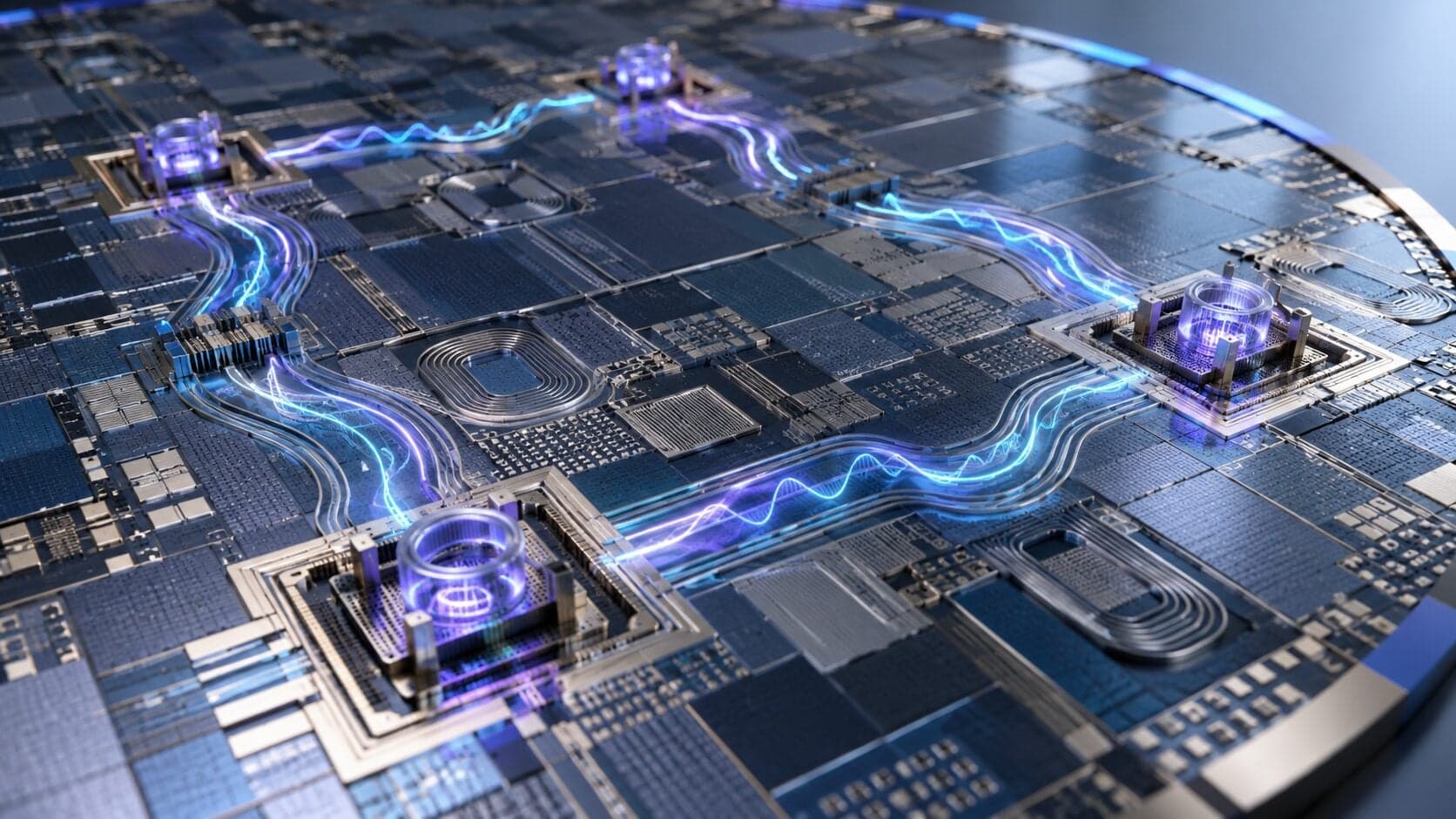
Imagine NVIDIA GPUs no longer needing a heat sink or cooling. Your smartphone never gets hot no matter how long you play a video game, and its battery lasts for days. It’s a distant promise, but it is inching toward reality.
Japan’s NTT is pursuing a fundamentally different approach to the power and bandwidth constraints confronting advanced computing, using photonics to replace electrical data movement in all chips, from AI data centers to consumer devices.
The technology is part of NTT’s IOWN (Innovative Optical and Wireless Network) initiative, which aims to combine conventional electronic processing with optical communications. It aims to replace electricity with light as a way of passing signals. NTT is targeting one of the increasingly important sources of energy consumption and latency: moving data between processors, memory and other components.
TSMC, Intel, Samsung and other chip fabricators have always addressed computing’s power problem solely by shrinking transistors, but it doesn’t change the fundamental way chips operate. Chips operate by sending electrons through microscopic copper wires, whether they are manufactured on a 10nm node or a 2nm node.
The problem is that every time an electron moves through a copper wire, it meets electrical resistance. The wire pushes back. The friction of pushing billions of electrons through microscopic copper pathways billions of times a second generates massive amounts of thermal energy.
For decades, the tech industry largely ignored this problem because, as transistors got smaller, travel distances decreased and resistance remained manageable. But as chips get down into the single-digit nanometers, the old fix of just shrinking transistors is no longer applicable.
Enter NTT, a 115-year-old telecommunications firm in Japan. It is developing what it calls the photonics-electronics convergence (PEC) architecture, which uses optical signals for high-speed data movement.
Optical communications offer a potential alternative because photons can transport data without the electrical resistance associated with conventional copper interconnects. That means faster data movement without heat.
The technology is being introduced in stages rather than attempting an immediate transition to optical consumer processors. Early IOWN deployments focus on connections between servers and circuit boards, where the power and bandwidth benefits can have an immediate commercial impact.
Optical interconnects could allow data to move between processors and memory at substantially higher bandwidth while reducing the energy required for communication. That is particularly appealing to systems built around high bandwidth memory and large numbers of AI accelerators.
The company’s earlier IOWN generations are focused on equipment-level and board-level optical connectivity. Future generations are intended to bring optical connections onto the motherboard and eventually into processor packages. IOWN 3.0 is targeted for roughly 2028–2029, while IOWN 4.0, which aims to integrate optical transceivers much closer to individual processor components, is planned for around 2032.
NTT’s strategy also has significant industry backing. Intel is a steering member of the IOWN Global Forum, while SK hynix has been working with NTT on optical memory technologies. That suggests optical interconnects are gaining traction across the industry.
The immediate market is likely to be AI and high-performance computing, where bandwidth and power requirements are growing rapidly. Consumer applications are considerably further away because of different design priorities and the challenge of adapting enterprise technology for compact, inexpensive devices.